
Quickly respond to customer needs



Feedback
FAQ
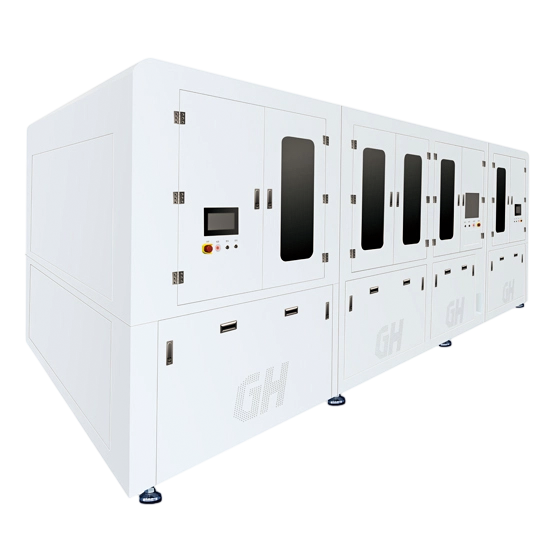
The wafer splitting machine equipment is used for the splitting process after laser cutting of wafers, with fully automated production. It can automatically identify and operate chips such as mirror, roughening, PSS, back metal plating, DBR chip processes, and ensure a splitting yield of over 98%.
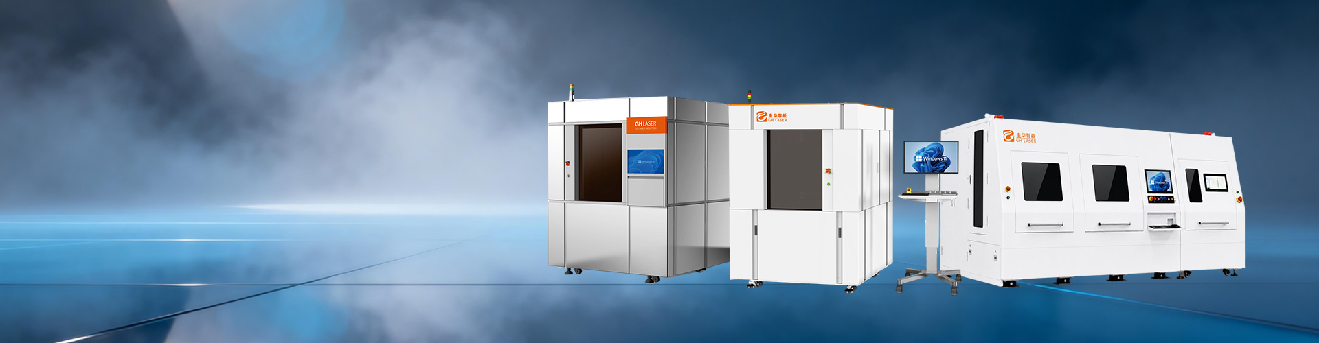
A cutting device developed for large-format transparent and brittle materials, with a cutting range of 600mm×700mm.
-
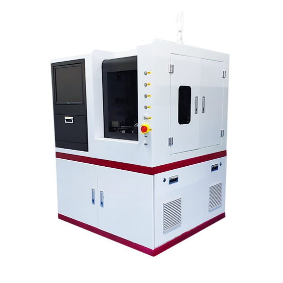
A cutting device developed specifically for carbon fiber materials, capable of cutting, drilling and grooving composite materials such as carbon fiber, glass fiber and Kevlar. It can handle materials with a thickness ranging from 0.05mm to 1mm, and is applicable to the processing of display backplanes, mobile phone back shells, AR glasses shells, etc
-
A cutting device developed specifically for carbon fiber materials, capable of cutting, drilling and grooving composite materials such as carbon fiber, glass fiber and Kevlar. It can handle materials with a thickness ranging from 0.05mm to 1mm, and is applicable to the processing of display backplanes, mobile phone back shells, AR glasses shells, etc
-
A cutting device developed specifically for carbon fiber materials, capable of cutting, drilling and grooving composite materials such as carbon fiber, glass fiber and Kevlar. It can handle materials with a thickness ranging from 0.05mm to 1mm, and is applicable to the processing of display backplanes, mobile phone back shells, AR glasses shells, etc
- Wide temperature-controlled process window, compatible with low to high temperature ranges; enables constant-rate etching to ensure stability and consistency in batch processing
- Long chemical solution service life, eliminating the need for frequent replacement and reducing operational costs
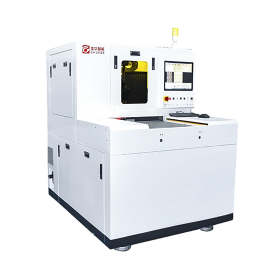
This device supports regular characters, one-dimensional/two-dimensional codes, and 59mm、1018Marking with mm dot matrix pattern. The marking font can be scaled based on SEMI standards, and the character content can be flexibly customized. It is equipped with dual modes of ID wafer edge marking and DIE single-chip independent marking, suitable for precision wafer marking processing.

